Strained Silicon On Insulator Wafers

Strained Silicon On Insulator
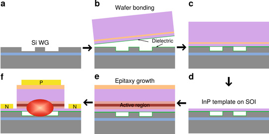
Indium Phosphide Template For Laser And Silicon On Insulator Integration

Breakthrough In Silicon Technology Wafer Level Strained Silicon Technology Announced By Sigen

Stretching Silicon S Lifespan Sciencedirect

Pdf Fabrication Of Silicon On Insulator Soi And Strain Silicon On Insulator Ssoi Wafers Using Ion Implantation

Products Soitec Soitec

Semiconductor wafer direct bonding combined with mechanical grinding of the donor wafer and chemical etching of the remaining silicon as well as the sige layer is an alternative to the hydrogen induced layer transfer hilt.
Strained silicon on insulator wafers.

Process Flow Of Fabricating Strained Silicon On Bpsg A Handle Wafer Download Scientific Diagram

Strained Silicon On Insulator Ssoi By Waferbonding Sciencedirect

Figure 1 From Impact Of Strained Silicon On Insulator Ssoi Substrate On Finfet Mobility Semantic Scholar

Strained Silicon On Soi Substrates Adds Up Ee Times
Source : pinterest.com
